NCP1606
http://onsemi.com
12
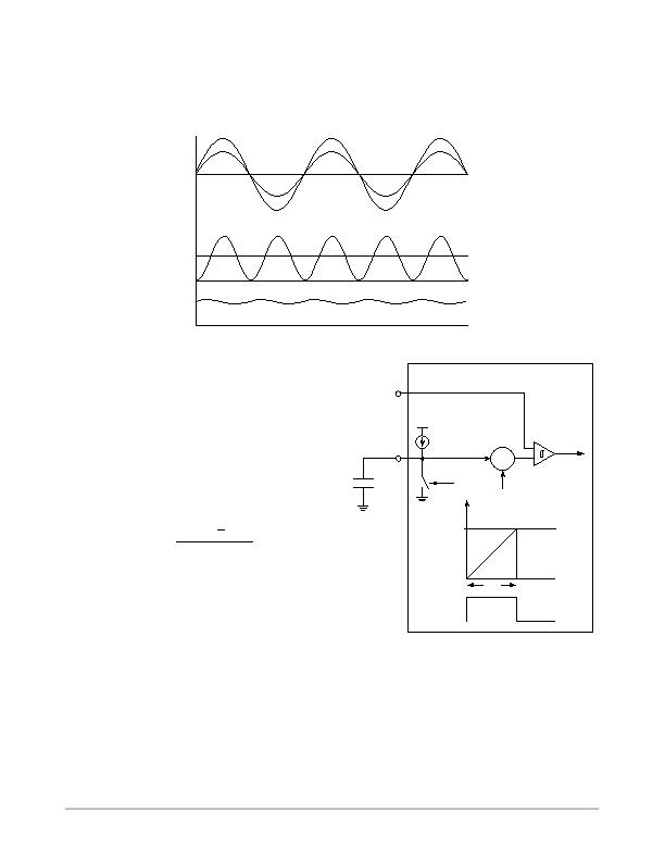
the average demand only. Therefore, the output capacitor
must
absorb
the difference between the delivered power
and the power consumed by the load. This means that when
the power fed to the load is lower than the demand, the
output capacitor discharges to compensate for the lack of
power. Alternatively, when the supplied power is higher
than that absorbed by the load, the output capacitor charges
to store the excess energy. The situation is depicted in
Figure 26.
Figure 26. Output Voltage Ripple for a Constant Output Power
V
OUT
P
OUT
P
IN
Iac
Vac
As a consequence, the output voltage exhibits a ripple at
a frequency of either 100 Hz (for 50 Hz mains such as in
Europe) or 120 Hz (for 60 Hz mains in the USA). This
ripple must not be taken into account by the regulation loop
because the error amplifiers output voltage must be kept
constant over a given ac line cycle for a proper shaping of
the line current. Due to this constraint, the regulation
bandwidth is typically set below 20 Hz. For a simple type 1
compensation network, only a capacitor is placed between
FB and Control (see Figure 1). In this configuration, the
capacitor necessary to attenuate the bulk voltage ripple is
given by:
C
COMP
+
10
G
20
4 @ p f
line
@ R
OUT1
(eq. 3)
where G is the attenuation level in dB (commonly 60 dB)
ON TIME SEQUENCE
Since the NCP1606 is designed to control a CRM boost
converter, its switching pattern must accommodate
constant on times and variable off times. The Controller
generates the on time via an external capacitor connected
to pin 3 (Ct). A current source charges this capacitor to a
level determined by the Control pin voltage. Specifically,
Ct is charged to V
CONTROL
minus the V
EAL
offset
(typically 2.1 V). Once this level is exceeded, the drive is
turned off (Figure 27).
Figure 27. On Time Generation
Control
Ct
+
PWM
+
DRV
I
CHARGE
t
ON
V
EAL
V
CONTROL
V
EAL
t
ON
V
Ct
V
Ct(off)
V
DD
DRV
V
CONTROL
Since V
CONTROL
varies with the RMS line level and
output load, this naturally satisfies equation 1. And if the
values of compensation components are sufficient to filter
发布紧急采购,3分钟左右您将得到回复。
相关PDF资料
NCP1607BDR2G
IC PFC CONTROLLER CRM 8SOIC
NCP1611BDR2G
IC PFC CTLR HE ENHANCED 8-SOIC
NCP1651DR2G
IC PFC CONTROLLER CCM/DCM 16SOIC
NCP1654BD133R2G
IC PFC CCM 133KHZ 8-SOIC
NCP1927DR2G
IC CTLR PFC/FLYBACK 16-SOIC
NCP380HMU21AATBG
IC CURRENT LIMIT SWITCH 6-UDFN
NCT1008DMT3R2G
TMP DIO MON/SMBUS 4CH 8WDFN
NCT210RQR2G
IC TEMP SENSOR LOC/REM 16QSOP
相关代理商/技术参数
NCP1606BOOSTGEVB
功能描述:电源管理IC开发工具 OSPI NCP1606 100 W BOOST
RoHS:否 制造商:Maxim Integrated 产品:Evaluation Kits 类型:Battery Management 工具用于评估:MAX17710GB 输入电压: 输出电压:1.8 V
NCP1606BPG
功能描述:功率因数校正 IC LO CST PWR FCTR CONT RoHS:否 制造商:Fairchild Semiconductor 开关频率:300 KHz 最大功率耗散: 最大工作温度:+ 125 C 安装风格:SMD/SMT 封装 / 箱体:SOIC-8 封装:Reel
NCP1607BDR2G
功能描述:功率因数校正 IC CST EFCT PW FCTR CTR RoHS:否 制造商:Fairchild Semiconductor 开关频率:300 KHz 最大功率耗散: 最大工作温度:+ 125 C 安装风格:SMD/SMT 封装 / 箱体:SOIC-8 封装:Reel
NCP1607BOOSTGEVB
功能描述:BOARD EVAL NCP1607 100W BOOST RoHS:是 类别:编程器,开发系统 >> 评估演示板和套件 系列:* 标准包装:1 系列:PCI Express® (PCIe) 主要目的:接口,收发器,PCI Express 嵌入式:- 已用 IC / 零件:DS80PCI800 主要属性:- 次要属性:- 已供物品:板
NCP1608BDR2G
功能描述:功率因数校正 IC COST EFFECT PWR FACT CONT RoHS:否 制造商:Fairchild Semiconductor 开关频率:300 KHz 最大功率耗散: 最大工作温度:+ 125 C 安装风格:SMD/SMT 封装 / 箱体:SOIC-8 封装:Reel
NCP1608BOOSTGEVB
功能描述:电源管理IC开发工具 NCP1608 100 W BOOST EVB PWR SPY
RoHS:否 制造商:Maxim Integrated 产品:Evaluation Kits 类型:Battery Management 工具用于评估:MAX17710GB 输入电压: 输出电压:1.8 V
NCP1611ADR2G
功能描述:功率因数校正 IC NCP1611A ENHANCED PFC
RoHS:否 制造商:Fairchild Semiconductor 开关频率:300 KHz 最大功率耗散: 最大工作温度:+ 125 C 安装风格:SMD/SMT 封装 / 箱体:SOIC-8 封装:Reel
NCP1611BDR2G
功能描述:功率因数校正 IC NCP1611A ENHANCED PFC RoHS:否 制造商:Fairchild Semiconductor 开关频率:300 KHz 最大功率耗散: 最大工作温度:+ 125 C 安装风格:SMD/SMT 封装 / 箱体:SOIC-8 封装:Reel